-///-
-///-
0. quickstart (under construction)
This work is intended as an adaptable, hardware-based Analogue High Definition Video Synthesis utility in the form of a Do-it-Yourself project.
It's aims are to provide:
these aims are pursued here as a cheap & simple DIY electronics project with:
Tradition states that if you're interested in video synchronization signals, you're either a specialized electrical engineer, or a video pirate trying to build a satellite descrambler. It follows that, in the world of do-it-yourself electronics, video-sync generation & reconstruction schematic information tends to be rather fragmented, incomplete, obscured. The great push to ditch analogue HD video in favour of digital techniques was in a large part promoted by the spectre of intelectual property piracy. To quote one internet forum user called paintit77, "Component is a very robust system with one problem, Hollywood can't control it." To the executive class, this "analog hole" was a fearsome sarlacc-pit whose primary goal was to eat money (or more specifically, to disappear tens-of-billions in imagined profits).
So the industry killed analog HD and promoted digital in order to protect its interests from piracy.
[...so how's that been workin' out for ya'..?]
I would maintain that technological advancements, particularly those backed by power, tend towards ideologically driven efforts at control and exploitation - a far cry from technical inevitabilities or quasi-religious adherences to the notion of progress-as-a-force-of-nature. As a video artist it should be enough to relax and enjoy the building of a sync-generator; and without the need to question (beyond mere technical utility) why one would want to build such a thing; or what our role in a sociopolitical, technological, and/or historical context would be. Personally, I think that we should be like Ursula Franklin and ask how specific technologies either prescribe our role within social hierarchies, or conversely, offer holistic relationships to production processes.
Displays and (analogue to digital) converters can be quite picky about synchronization. In some parameters you have to be pretty tight, but some tolerances are quite lax. With sync pulse-widths and the timing of blanking periods there tends to be a lot of wiggle room in terms of getting and maintaining a stable picture – most equipment seems to be quite forgiving. In terms of the ratio between H and V frequencies, I've found it works best to be strict about this – that is if your goal is to form a good working relationship between your experiments and your chosen display technology.
I would consider this a novice to intermediate electronics project. An oscilloscope and/or a frequency-counter are not needed for building and testing one of these sync-generators,
but they're useful, fun, educational, and rather easy to find 2nd-hand (cheap). Be sure to have a multimeter.
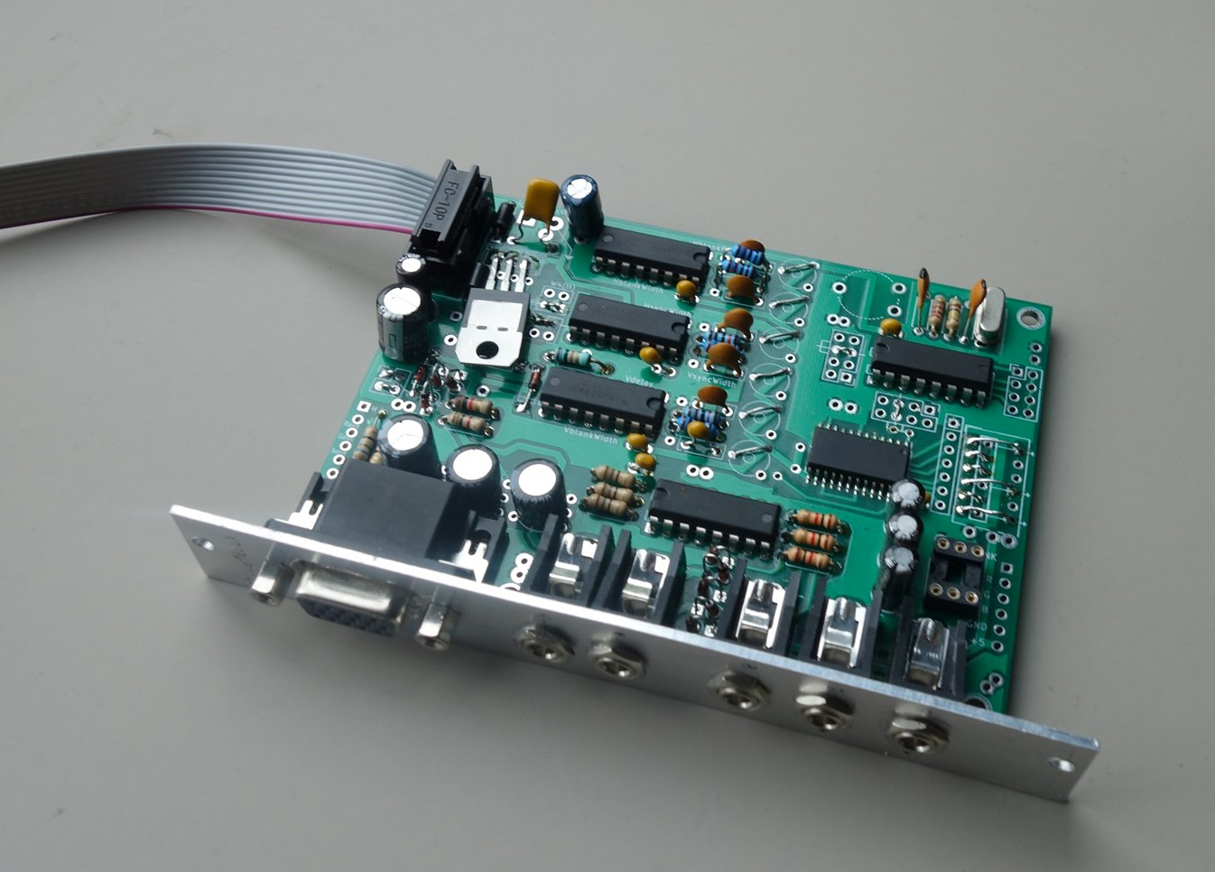
This DIY project is well thought through, though is well far from perfect. It is simple or complex depending on a) your perspective and b) how you'd like to configure it.
Some examples of various possible configurations and iterations are provided in this publication.
-///-
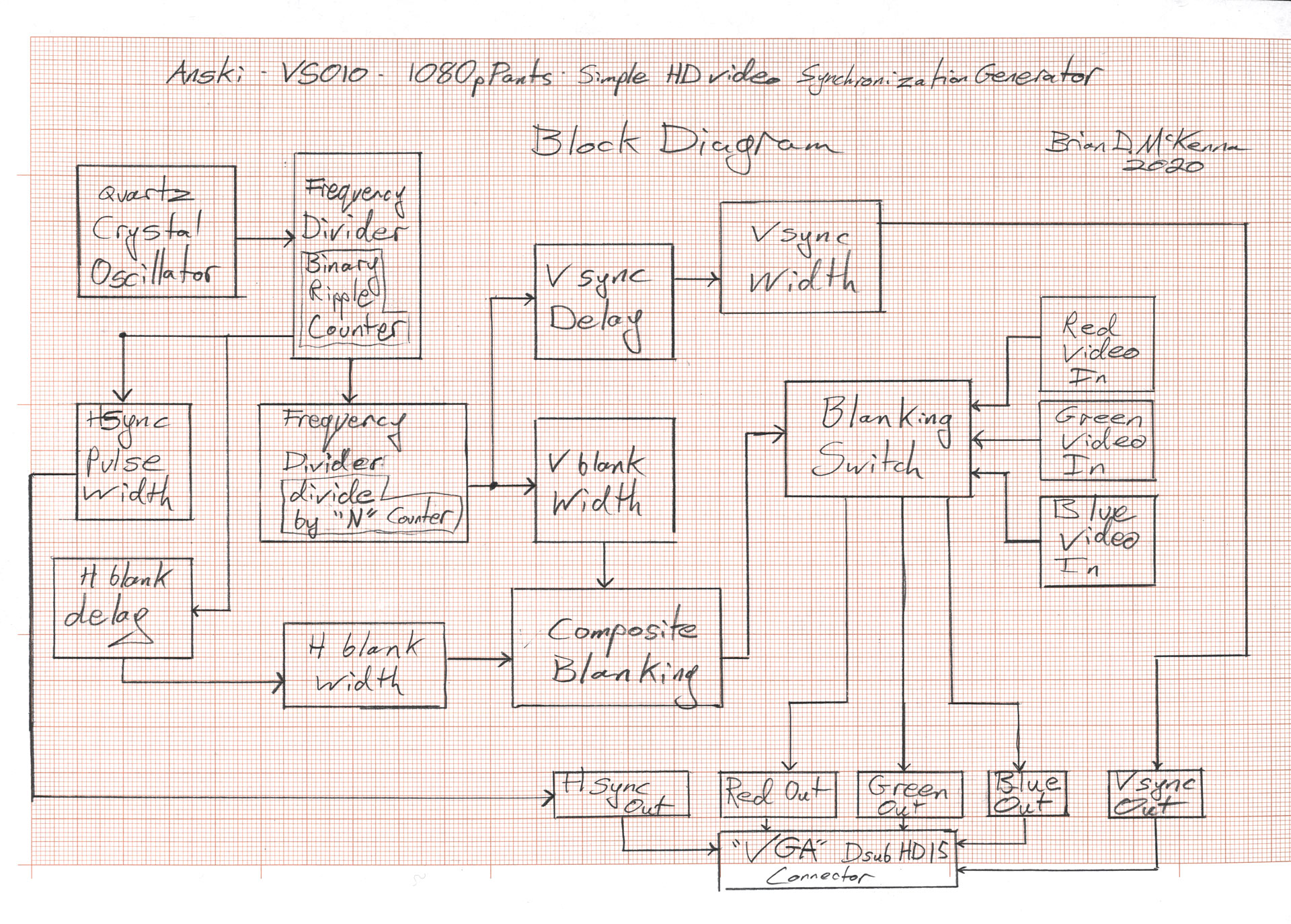
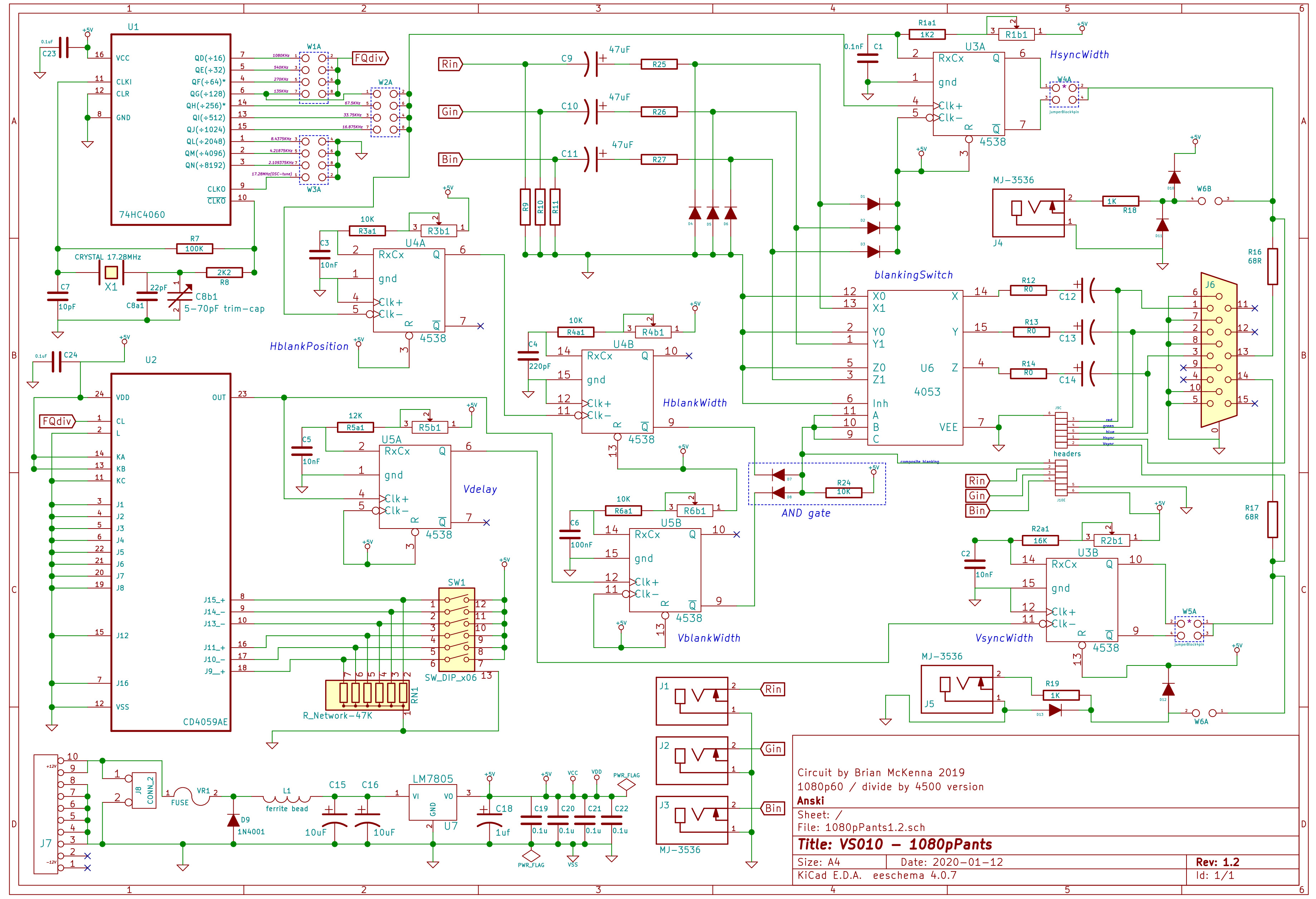
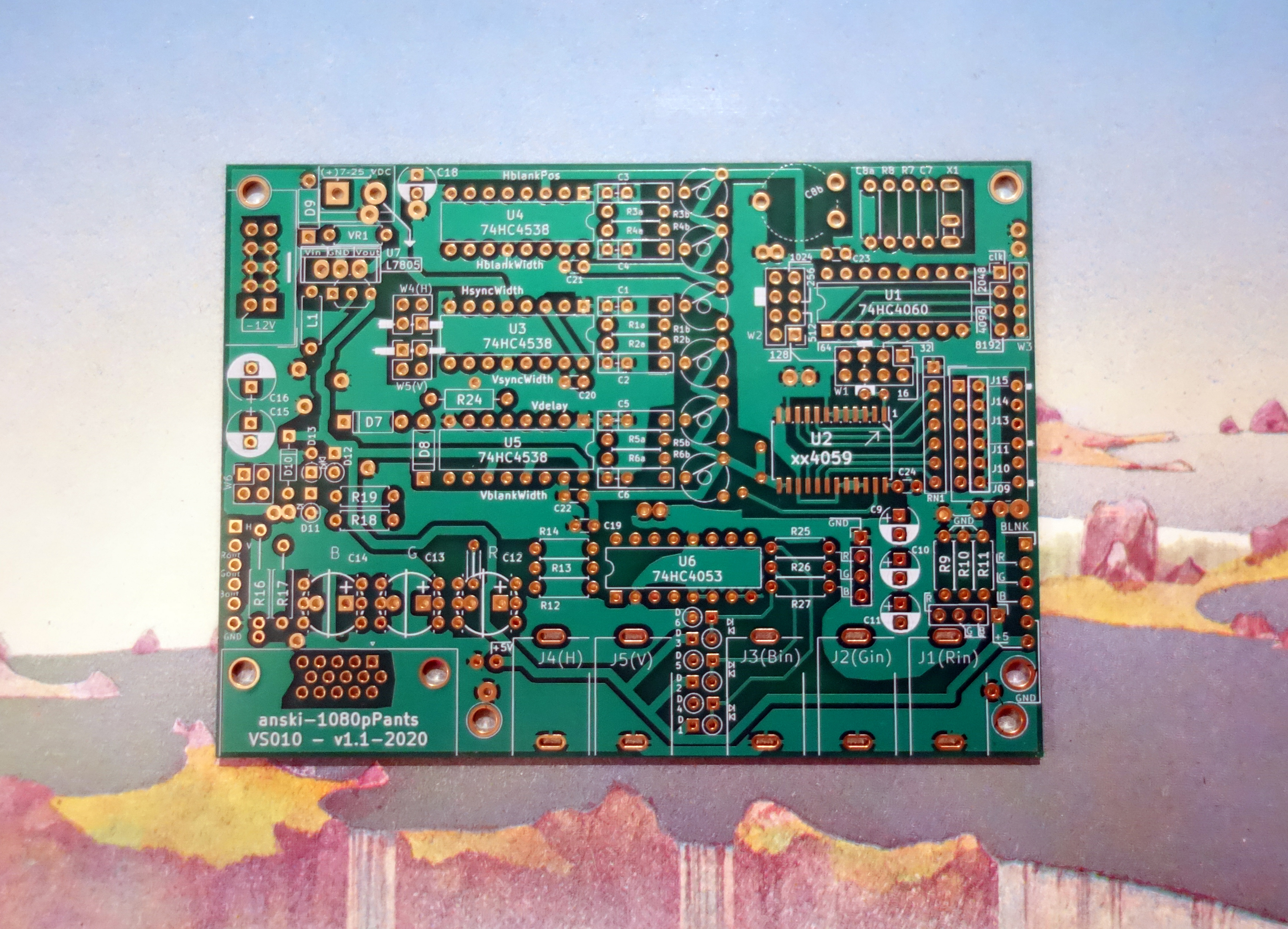
A quartz crystal oscillator generates a stable high-frequency clock. This clock is divided down to our horizontal sync frequency with a binary-ripple-counter. One of the ripple-counter's outputs is further divided down to our vertical sync frequency with a divide-by-n-counter. An array of 'one-shots' is used to set our horizontal and vertical synchronization pulse-widths, and for setting the timing of our blanking periods. Through an AND-gate, our horizontal and vertical blanking signals are combined into a single composite signal; this is used to gate a 3-channel video-blanking switch.
It should be obvious, but for reference:
The sync-generator 'core' of this design is quite simple:
-///-
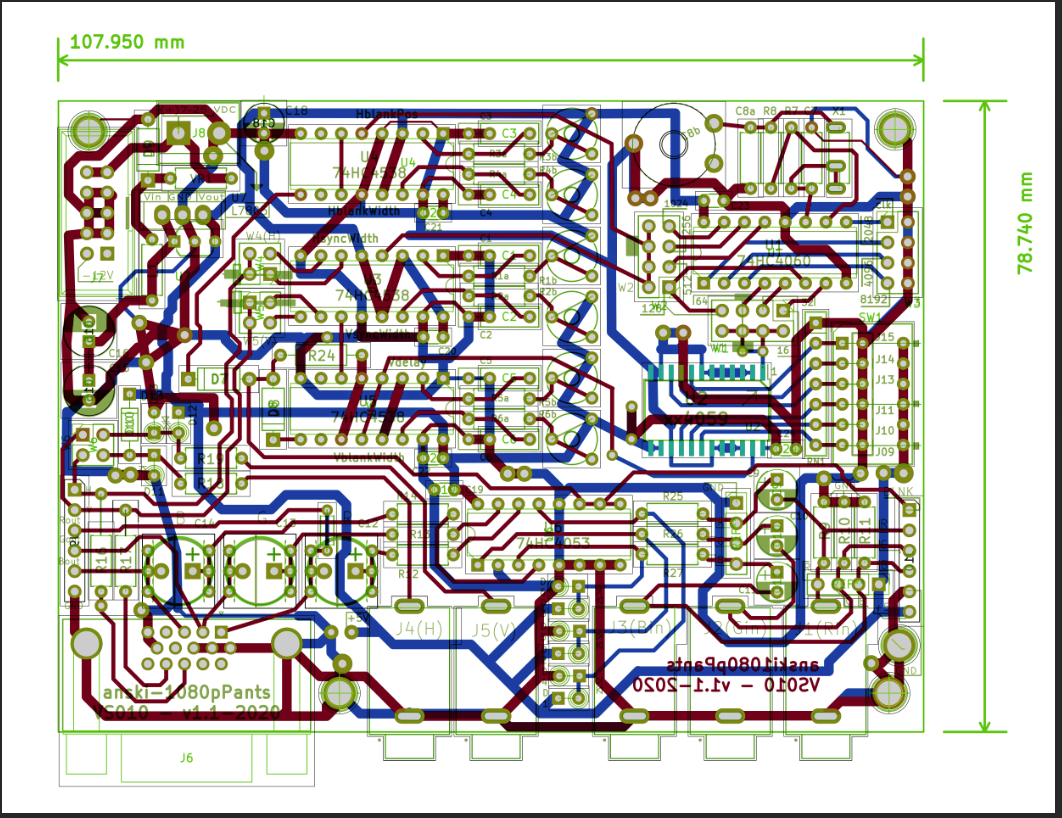
The schematic here represents the configurability of this project's PCB to a large extent; so to that end, it starts to look quite busy. A number of 'optional extras' are included, and these can be omitted as required. W1-W5 for example: These are jumper-blocks; they can be left off and specific connections just hardwired when adaptability to multiple formats, internal test-patterns and other bonuses are not needed. The same holds true for the DIP-switch marked SW1, it's just for switching between different video formats; if omitted, the RN1 resistor-network would not be needed either.
6 trim-potentiometers: R1b - R6b, can help with precision and adjustability - they can be very handy - but they are not strictly needed for a perfectly functioning circuit; a jumper-wire or a second fixed value resistor can be installed instead.
C8b is a trimable capacitor: This is for 'pushing', 'pulling', or otherwise fine-tuning the frequency of the quartz crystal (X1); this could be most useful for operating at 29.97 frames-per-second instead of 30 frames per second. Again, the circuit will function properly without it.
Examples of how to build some specific implementations are covered elsewhere in this publication.
Since 1080p60 is quite a versatile, widespread, and established HD video standard, it is treated as a default format for the purposes of this schematic.
Denoted frequency values and jumper setting marked with (*), and DIP switch settings marked with (+) or (-) reflect this 1080p60 default. The stated quartz crystal frequency value of 17.28MHz in this drawing is specific to 1080p60.
Resistors R1-R6, in combination with capacitors C1-C6 control the timing and pulse-widths of H/V synchronization and blanking signals. So it follows that the stated values of R1-R6, and C1-C6 are also specific to a 1080p60 format here.
Jumpers W1 & W2 could be changed to select 1080p30 with a 17.28MHz crystal, but R1 - R6 would need to be changed also. [provision for installing DIP sockets on the PCB allow for the quick-changing of resistors and capacitors]
If a 576p50 format is required for example, a 4MHz crystal could be used in combination with corresponding W1 & W2 jumper settings, corresponding DIP-switch settings, and corresponding values for R1-R6 & C1-C6.
The same format could also be derived from a 16MHz crystal by using different W1 & W2 jumper settings – thus horizontal frequency comes from dividing by 16MHz by 512 to get 31.25KHz instead of dividing by 4MHz by 128 to get 31.25KHz; and vertical frequency comes from dividing 16MHz by 64 and then 5000 (via U2) to get 50Hz instead of dividing 4MHz by 16 and then 5000 to get 50Hz.
In the 'formats' section, specific settings for crystal frequencies, resistors, capacitors, jumpers, and the DIP-switch are provided for a variety of HD and SD video standards.
CD74HC4060 – High Speed CMOS Logic 14-Stage Binary Counter with Oscillator
The magic of magical crystals
Quartz crystal X1 is used to set U1's built-in pierce-oscillator to the “master clock” frequency of our circuit. R7, R8, C7, and C8a1 are needed to get the crystal to function properly; the values can change a bit depending on the requirements of specific crystals. C8b1 is an optional variable capacitor to help with (besides some fine-tuning) pushing or pulling the oscillator frequency a bit.
Working at 29.97 frames/second instead of 30 is an example of wanting to do that; there's practical limits to how far you can go with such things and there can be quite some 'pullibility' variation in differently manufactured timing crystals.
The binary ripple counter section of U1 divides our master clock down to the frequency of our horizontal synchronization pulses – and to the frequency we'll send to U2. W1 and W2 are 8-pin, 2-row pin-headers used as jumper-blocks for selecting specific frequency divisions and passing those on to further stages in our circuit.
W1 selects the input frequency of U2 – the divider which produces our vertical refresh clock.
W2 selects which frequency will be our horizontal clock (line frequency) and is passed onwards to the inputs of U3a and U4a.
These jumper blocks are optional but largely recommended – being able to quickly change frame-rate and line-frequency can be a very handy feature (for changing from from 1080p60 to 1080p30 for example). W3 is even more optional, it outputs the leftover frequency division outputs of U1, these can be handy for clocking other circuits in a video synthesizer system. Connected to W3 is pin9 of U1, here you can effectively measure or further exploit the master frequency of U1’s oscillator. It’s quite easy to disturb our circuit’s oscillator function by playing around with U1 pin9 too much – so be aware of that sensitivity.
You don't need to use U1's built-in oscillator; the CD74HC4060 can lock to an external clock applied to pin11 – very handy for certain uses.
U2 is a divide-by-n-counter in the form of a CD4059 or CD74HC4059.
This is used to divide the (W1) output of U1 down to our system's vertical refresh rate.
What is essentially going on here is the horizontal refresh rate is being divided by the total number of video lines;
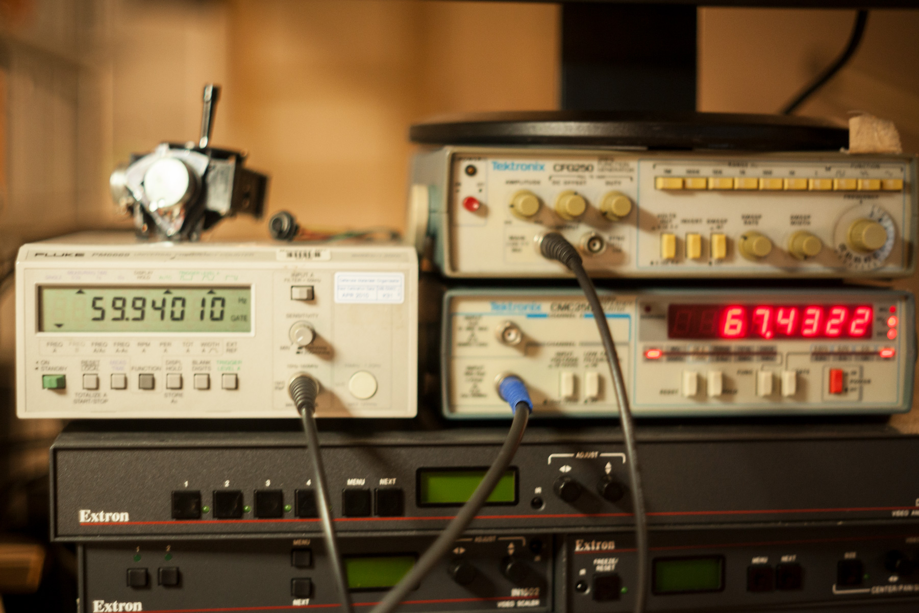
in the case of 1080p60: a horizontal line rate of 67.5KHz is divided by 1125 total lines to get 60Hz.
1125 total lines is 1080 lines of active video + 45 lines of blanking (front-porch + sync + back-porch)
17,280,000 / 256 = 67500 / 1125 = 60
So for the default values of the schematic:
In our case of U2:
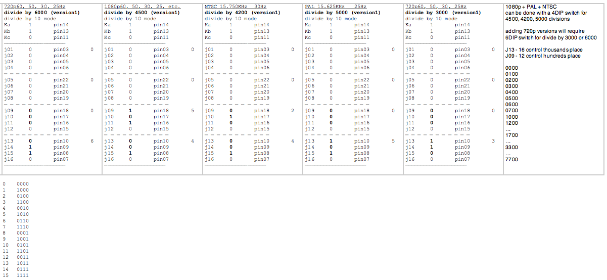
pin14(KA), pin13(KB), and pin11(KC) program the divide-by mode; our schematic's default is divide—by–10(ten)–mode. Tying Pin2 to ground keeps ‘latch mode’ switched off. Pin1 is our clock input and pin23 is our divided clock output [it's one short output pulse for every 4500 input pulses on our schematic's default]. Pins 3-10 and pins 15-22 are the ‘jam inputs’ used to program which integer the input clock will be divided by.
Connecting pins 8, 16, and 18 to +5volts and everything else to ground will produce divide by 4500 if we’re in divide-10-mode.
(again, check out the datasheet for more info on what going on here)
SW1 is an optional 6way SPST DIP-switch connected to U2’s pins 9-11 and 13-15. This can be used to change our divide-by-number to a variety of different ‘jammed’ presets.
Pins 9, 10, and 11 set the hundreds place of our divide-by-number to anything from 0 to 7 by setting 3bits of a 4bit word.
Likewise, pins 13, 14, and 15 set the thousands place of our divide-by-number to anything from 0 to 7 by controlling 3bits of a 4bit word.
RN1 is an integrated set of 6 resistors (47K) which allow the SPST DIP switch to select between +5(1) and GND(0)
--> on or off <--
for each connected jam-input pin.
RN1 could just be replaced by discrete resistors.
Further, if only one frequency division setting for U2 is needed, jumper wires can be used to hardwire a given divide-by number and thus forgo the use of a DIP switch altogether.
U3A and U3B represent the two sections of a Dual Retriggerable Precision Monostable Multivibrator. The 74HC4538 has been chosen due to its high-speed and short minimum pulse-width characteristics; the HCT4538 should be more or less interchangeable, however, variants such as the CD4538 or HEF4538 are really a different animal. U3A sets the horizontal-synchronization-pulse-width(Hsync) and U3B sets the vertical-synchronization-pulse-width(Vsync). The combination of C1 and R1a sets the timing of Hsync’s pulse-width. C2 and R2a do the same for Vsync. R1b and R2b are optional trim-pots which allow for more precise tuning of Hsync and Vsync pulse-widths – high precision seems generally not necessary however. Fun-fact: choosing between the “Clk+” or “Clk-” inputs selects either rising and falling edge triggering; the unused input needs to be tied to +5 or GND depending. W4 and W5 are jumper-blocks which can be used to select positive going or negative going Hsync and Vsync outputs – different video standards are known to use different combinations of positive or negative sync pulses. These jumperblocks can be omitted and the correct connection hardwired if only one video standard is needed. [1080p60 most generally requires Hysnc and Vsync to be positive]. The H&V sync signals are brought to our Dsub15 (“VGA connector”) J6 output via R16 and R17 which should be 68ohms; it’s a value which brings us to a good output impedance in combination with the inherent output impedance of U3.
Hsync and Vsync can be additionally routed to outputs J4 and J5 via jumper-block W6. With no jumpers installed, W6a and W6b could be used (via dunlop cables) to make any signals from jumper-blocks W1, W2, W3, W4 or W5 available to connector jacks J4 and J5 as outputs. The idea here is to allow the clocking (sync-ing) of other external circuits / modules / experiments to any subdivisions of our master-clock. J4 and J5 are indicated to be MJ-3536 jacks; also known as thonkiconn jacks, or 3.5mm mono minijack connectors as in eurorack standards.
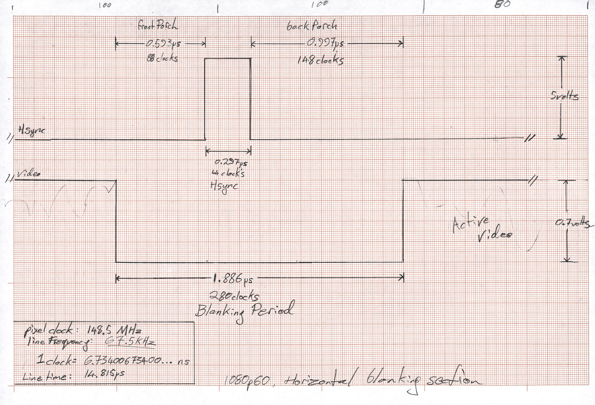
Video signals must be properly blanked out to zero volts for a period before and after the horizontal and vertical synchronization pulses in order to be displayed properly [see timing diagram].
U4 uses another Dual Retriggerable Precision Monostable Multivibrator chip to generate a horizontal blanking period based on the timing of Hsync.
U4a receives its trigger one half a line after U3a's trigger – so when the same output from U1 transitions to negative (50% duty-cycle).
C3, R3a (and optional R3b) set the delay timing of Hblank so that it will occur just before the next Hsync pulse – this creates a ‘front porch’ [see Hblank Timing-Diagram].
The output of U4a is fed to the input of U4b which uses C4, R4a (and optional R4b) to set the width of our horizontal blanking period.

Vertical blanking is generated here in much the same way as Hblank. However, setting a delay of almost one frame, or even half a frame can become quite an invitation for jitter. For this reason I elected to delay Vsync a little bit – so that it occurs within the Vblank period (as it should). U5a delays Vsync as timed by C5, R5a (and optional R5b). U5b sets the duration of Vblank with C6, R6a (and optional R6b).
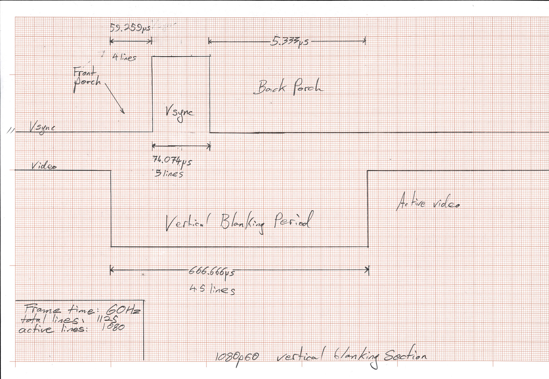
[drawings are to (temporal) scale]
Hblank and Vblank need to here be combined into what’s generally referred to as composite blanking. This is done with an AND gate such that either an Hblank pulse or a Vblank pulse can be used to essentially switch-off our video signals at the appropriate times. A single AND gate is easy to make with discrete components – D7, D8, and R24 create composite blanking and use this to control U6’s switches.
Three-way analogue switch U6 is a 74HC4053. With a frequency response of 170MHz, some might say that this switch is inadequate for HD video.
They’d be right, however, this circuit isn’t geared towards seamlessly reproducing an HD video source input;
we don’t need all the headroom of 500MHz+ components for many, more abstract picture oriented applications.
Interpreting the schematic diagram here: pin11 is the controller of switch A; this toggles the connection of terminal X (pin14) to either X0 (pin12) or X1 (pin13). So X1 is our RED input, X0 is GND (blank), and X is our RED output.
And likewise, switch B (pin10) controls the Y channel and C (pin9) controls the Z channel.
Note that switches A, B, and C could be controlled independently, but they are chained together for the purposes of this circuit.
X1, Y1, and Z1 are our RGB video inputs.
X0, Y0, and Z0 are tied to ground, and so that is what our RGB outputs will be seeing during our blanking periods.
I have yet to investigate this in any detail, but applying a voltage other than zero volts to X0, Y0, and Z0 in such a setup could perhaps be used to manipulate the black levels of our video signals.
Standard L7805 or LM7805 voltage regulator and associated components. This takes a +12VDC input and supplies a regulated +5VDC to the circuit. The PCB includes footprints for using either a TO-220 or smaller TO-93 package as in the 78L05, 100mA version. D9 is for reverse polarity protection (accidentally pluggin the power in backwards), L1 is for filtering out high-frequency noise, C15 and C16 are for smoothing voltage ripples, as is C18. C19 - C22 are standard 0.1nF power decoupling capacitors which as a rule are placed as close as possible to the power-supply pins of each IC. VR1 is an over-temperature fuse which is optional and could be replaced with a jumper-wire.
R15 is missing, think of this like a missing 13th floor. R20, R21, R22, R23, R24 are also missing, think of this as a mistake. Alternately, if you choose to substitute RN1 for 6 discrete resistors, then just think of theirs numbers as R20, 21, 22, 23, 24, and R15.
J1 - J3 are the RED, GREEN, and BLUE inputs respectively.
J4 & J5 are connected to jumper-blocks W6-B and W6-A. With a jumper installed, J4 will output Hsync through R18. Consider the stated value of 1K as an error in the schematic drawing; a 56ohm resister will serve you much better.
Dunlop cables can be used with W6 to output signals from W1 - W3.
J6 is a standard High-Density-Dsub15 (VGA) connector which carries RGB video + Hsync & Vsync
For J7, a 10pin Eurorack pin-header can be used to apply +12VDC to the circuit, or the other directly connected 2pin power input footprint can be used with any power jack that will fit.
J9 & J10 are pin-headers for suppling RGB inputs, RGB output, Hsync and Vsync, Cblank (+5V power and GND also) to other circuit-boards in an expanded system.

—————————————————————————————————————
—————————————————————————————————————
To order a PCB, please send an email to pcb@recordingmedium.com
subject including "VS010 v1.1"
At this time, the price for one PCB is €10 + shipping.
A PCB with the SMD chip (U2 - CD5059) preinstalled is possible but costs €25.
Shipping is once / week on tuesdays.
Payment can be done through paypal to brian@mediumrecords.com
It should be noted that this circuit does not buffer or amplify video signals. In brief, what this means is:
I have built several iterations of this circuit for various different purposes.
Documentation of some of these will be inserted to this section.
Minimal and maximal approaches to building up one of these PCB's is covered with various details above; namely, what components can be left off and what can be added.
some examples could include:
—————————————————————————————————————

The above iteration configured to UXGA format; pin-headers and DIP switches installed for multi-format use; component sockets for adjusting sync-width and blanking timing adjustment; trim-pots for Hblank fine-tuning; input & output capacitors C9 - C14 omitted for DC coupled video input and output (wires installed instead); trim-cap C8b not installed; 6pin component socket for R25, R26, and R27 video signal input resistors. Protection diodes D1 - D6 & D10 - D13 not installed.
—————————————————————————————————————
The component values associated with a number of formats and some detailed timing information can be found here:
>> format-settings-1.1-1080pPants.html <<
—————————————————————————————————————
—————————————————————————————————————